The M190 is an entry-level wireless mouse made by Swiss computer peripherals giant Logitech. I bought this a couple of years ago to use with my laptop. It’s an OK mouse, although it feels quite plastic-y and the lack of forward/back buttons is a bit annoying. A while ago the scroll wheel developed an annoying habit of randomly scrolling up or down one line, so I decided to get rid of it and buy a new mouse. Of course, in my house I never throw away any electronic device without dissecting it first, so that’s what I did in this case, too.
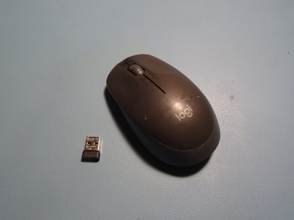
The design is very basic: just a plastic shell with two buttons and a scroll wheel. Rather than using Bluetooth, it connects to your computer through a proprietary wireless protocol known as Unifying. The mouse comes with a small Unifying dongle, which can also be used for other things like keyboards.
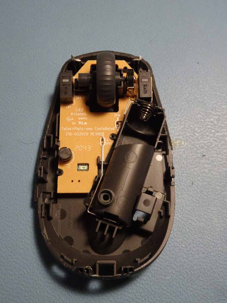
Inside the mouse we find one single-sided PCB. It’s quite rare to see these nowadays: multi-layer PCBs are so common that the cost difference is tiny. But every cent counts in in a low-cost, large-volume product like this, so it was apparently cheaper to use a couple of zero-ohm resistors instead of routing signals on two layers.
Apart from the obvious microswitches we also find an inductor, used to boost the single battery’s voltage to something like 3.3 V, and a cut-out showing the LED for the motion sensor. I don’t know why this cut-out was made, because the LED doesn’t shine upwards.
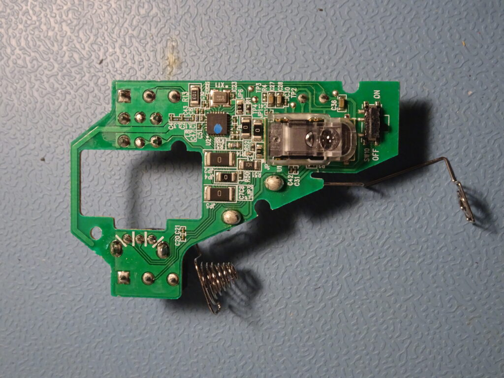
On the component side we find one 24-pin chip in a QFN package, a crystal oscillator, the optical motion sensor with its lens, an on/off switch and various passive components including a number of pretty large zero-ohm resistors. The battery contacts are held in place by two rather ugly blobs of solder. All the way on the left is a long trace that forms the 2.4 GHz antenna.
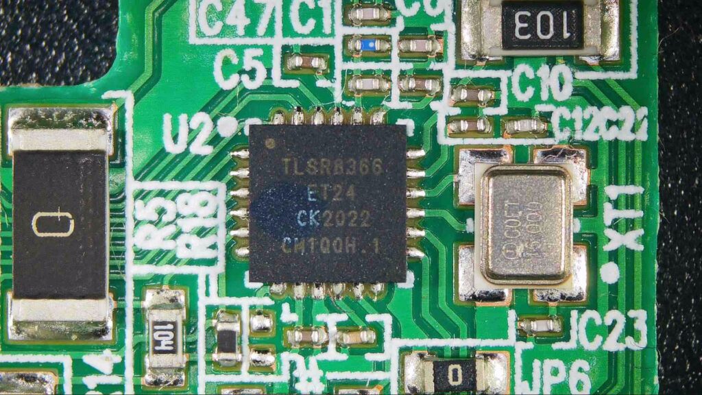
The main chip is a TLSR8366, which is a 32-bit microcontroller with an integrated 2.4 GHz transceiver. It’s made by Telink Semiconductor, a fabless manufacturer from Shanghai specialising in microcontrollers and RF chips.
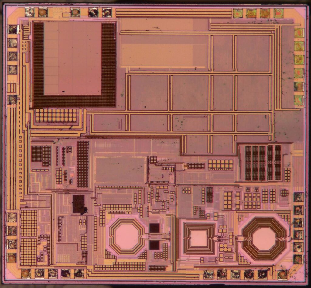
The chip looks pretty much as expected. We find large areas of automatically-generated digital circuitry along with a memory area in the upper left corner and RF circuits in the lower right.
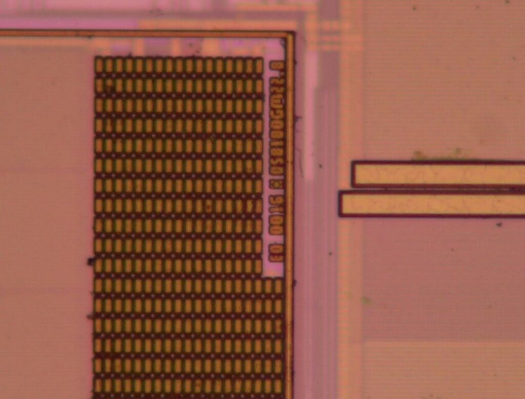
There’s not much identifying information to be found on the chip. The only bit is found here: “E0 0016 * 058180GM22.8” if I’m reading it correctly.
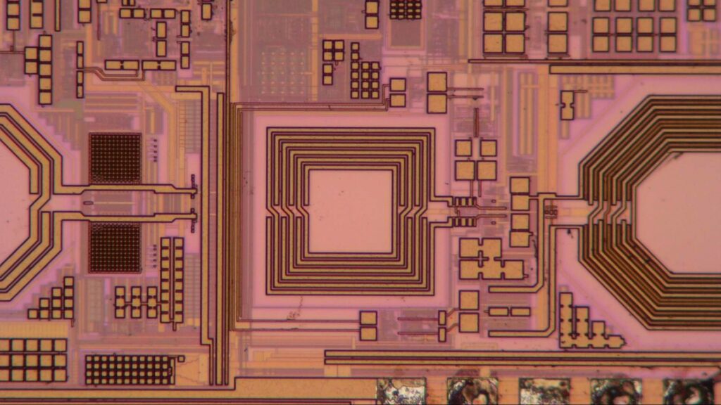
You can easily tell where the 2.4 GHz radio circuits are: on-chip coils like these are only used for RF work. Typically, one is used in an LC-type circuit for the local oscillator (likely the one on the left here), while the others are used for filtering and antenna matching.
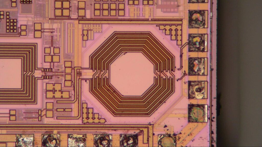
The coil in the right is clearly a transformer: we see two wires coming in on the left and two other wires going out on the right. The datasheet mentions that the RF transceiver has an integrated balun and a single TX/RX port, so that’s what we’re looking at here.
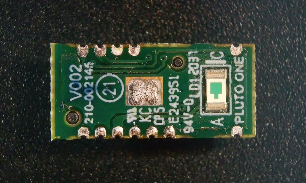
The image sensor is sitting on a small daughterboard mounted on the main PCB through castellated edges. There’s a whole bunch of model codes printed on it, the coolest being “Pluto One”. We also see the LED again that we saw through the hole in the main board.
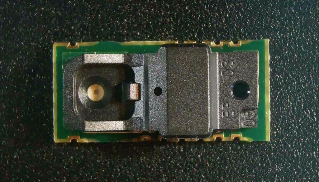
On the other side there’s a thick piece of black plastic. The LED shines through a hole in the left, while the camera looks out the tiny hole in the middle. There was also a lens mounted between this bit and the bottom of the mouse’s housing.
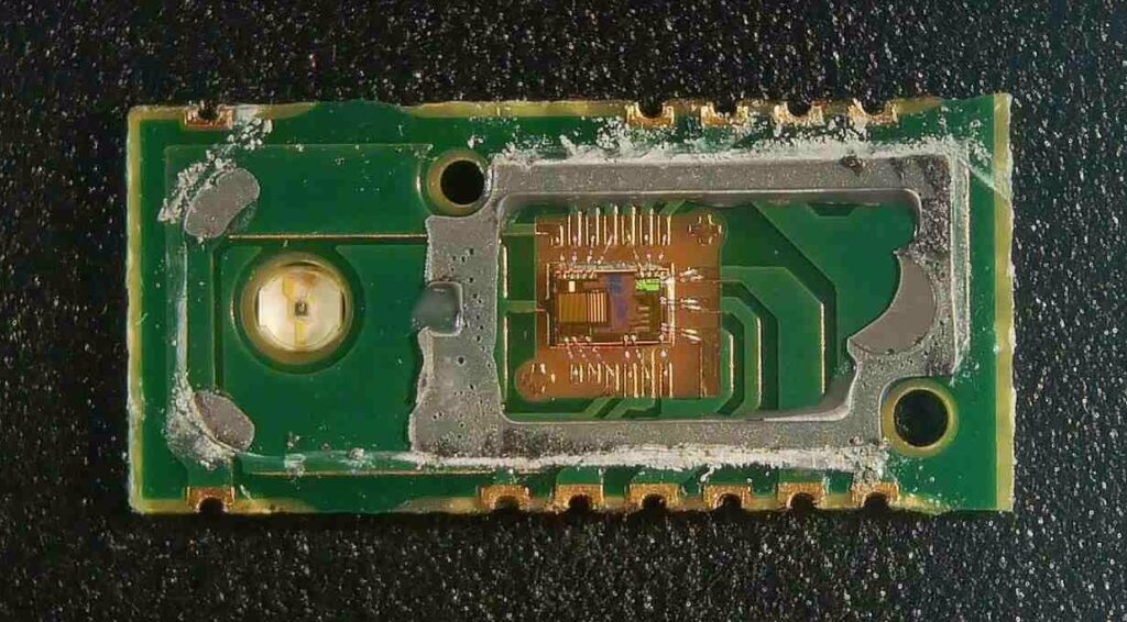
With a bit of persuasion, the black cover pops off, revealing a sensor chip directly bonded to the board.
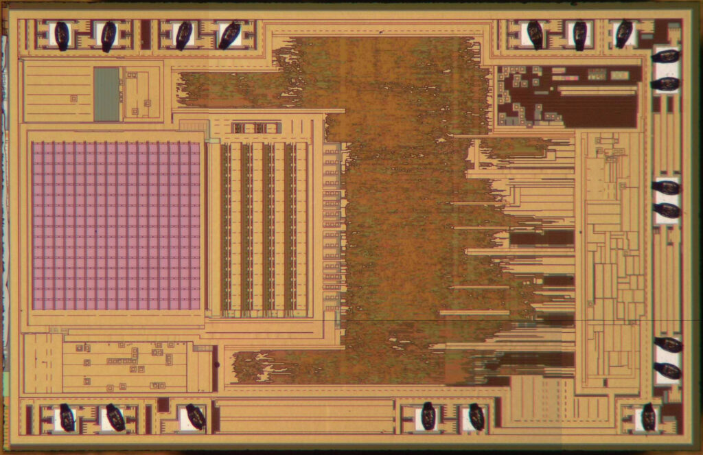
The chip contains a 16×16 pixel image sensor and lots of digital processing. It’s made in a rather modern process, judging by the amount of filler metal on the top layer.
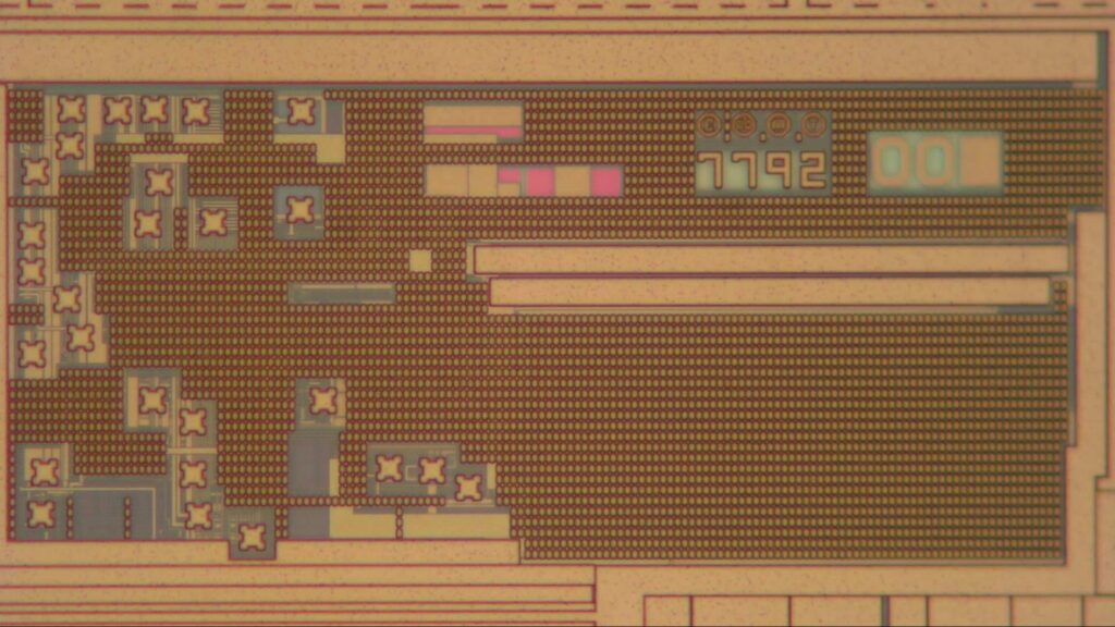
The only identifying features are the number 7792 and a few characters above it: next to the copyright and mask work symbols we find both a T and the letters “eb” in a circle. None of this seems to point to any manufacturer name or model number.
Also interesting are all those little X-shaped metal features. Given their location on the top metal layer I would assume these are test points, although I’ve never seen them in this shape: they’re usually square.

If we zoom in a bit more, we discover quite a bit of circuitry lurking below the X shapes and the filler squares.
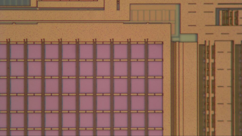
The pixels making up the image sensor seem to be simple squares. Most likely these form a charge-coupled device (CCD), an array of MOS capacitors that are read out in sequence.
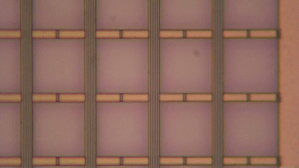
Even at the highest magnification level there are no further details visible, other than a few wires running in the vertical direction.
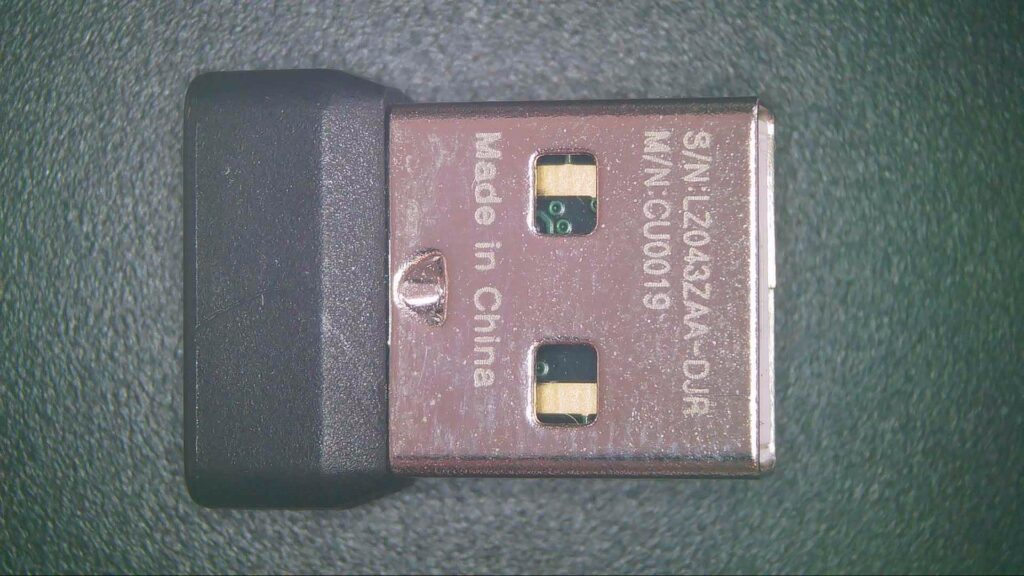
The dongle apparently has model number CU0019. Through the holes we can already tell that inside of the USB plug is a two-layer PCB.

Once we remove the outer packaging we’re left with this tiny circuit board, held in place by a white plastic frame. The board itself is razor-tin: just 0.5 mm.
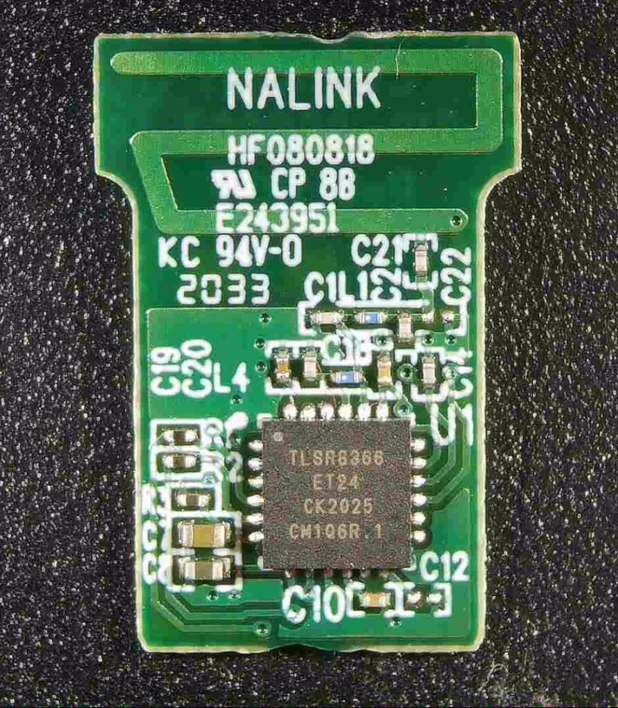
On the other side we find a TLSR8366 again. There’s a couple of passive components surrounding the chip as well as an S-shaped antenna at the top. Telink’s datasheet has an application example for a USB dongle on page 71, and it wouldn’t surprise me if the design we see here is similar if not identical to that in the datasheet.
