The ADXL345 is a MEMS accelerometer made by Analog Devices. It’s a popular device among hobbyists because of its low cost, easy availability and rich feature set. But apparently you should be careful about where you buy them: one of my readers ended up with a bunch of ADXL345s that had significant offsets, measurement axes that didn’t work at all, and an inoperative freefall detection mode. After spending lots of time trying to get them to work, he decided to send them to me instead and hopefully find out what was wrong with them.
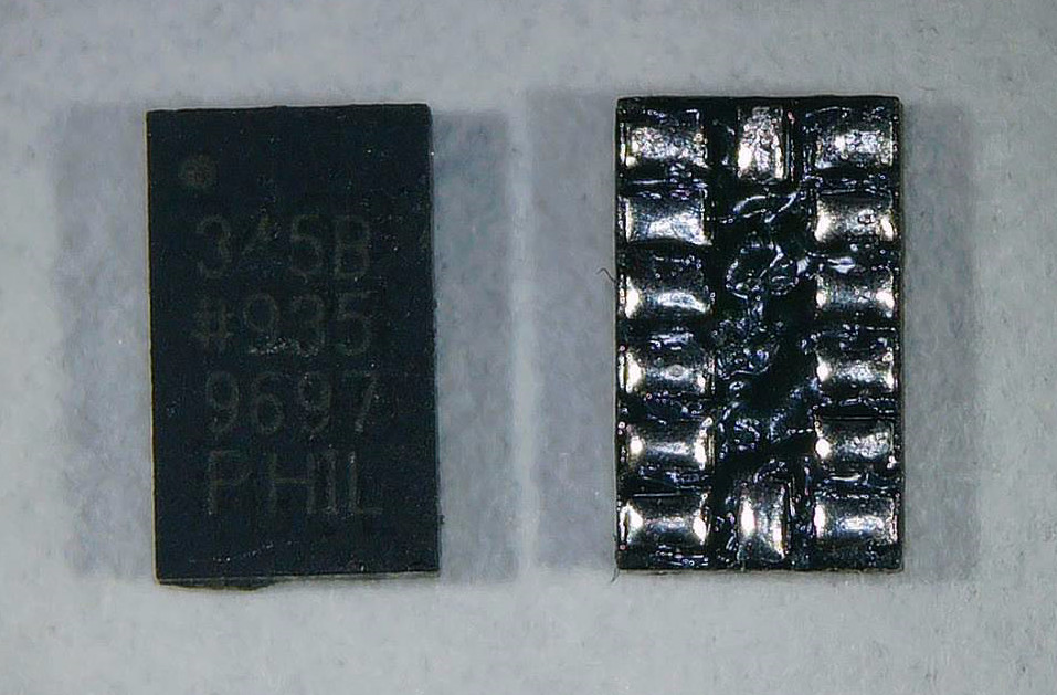
The front and back look pretty normal at first glance. But if we slightly change the illumination angle, we can already spot something unusual.
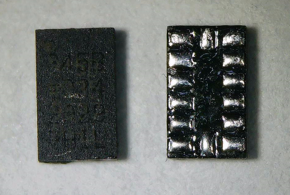
Behind the printed markings we find another set of laser markings. The top and bottom lines say the same thing (“945B” and “PHIL”), but the two lines in the middle are slightly different: “#934” instead of “#935”, and “2029” in place of “9697”. These numbers indicate things like the manufacturing date, a batch number or a factory indentifier and don’t affect the functionality or performance of the chip. However, the fact that there was a first set of numbers which was apparently deleted and replaced by another set is not a good sign. It could mean that this chip was part of a faulty batch meant to be destroyed, but ended up in the hands of an unscrupulous dealer who re-marked the top side and sold them as good parts.
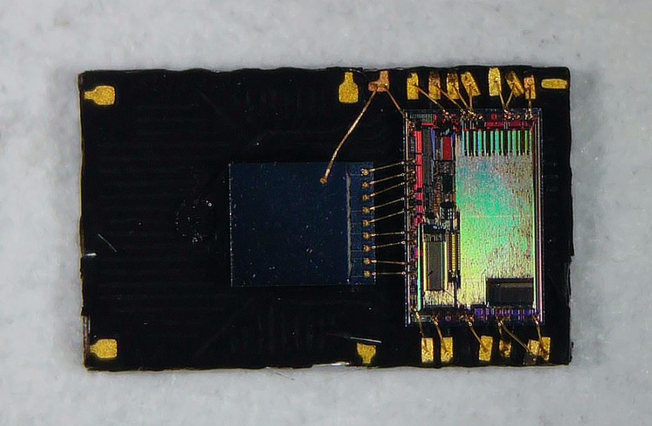
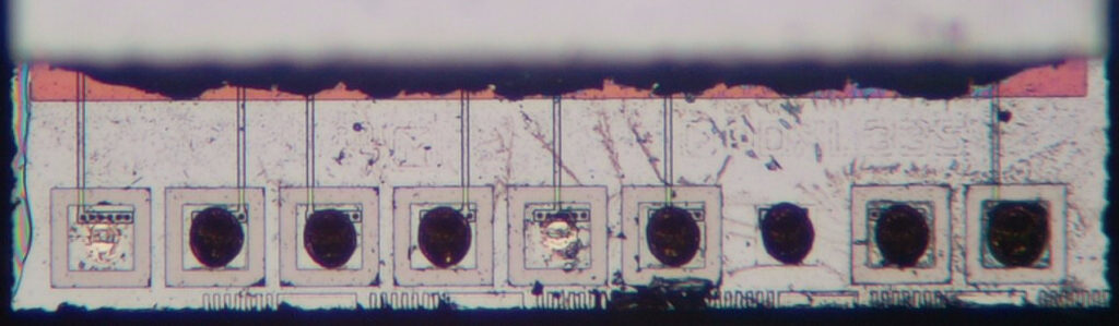
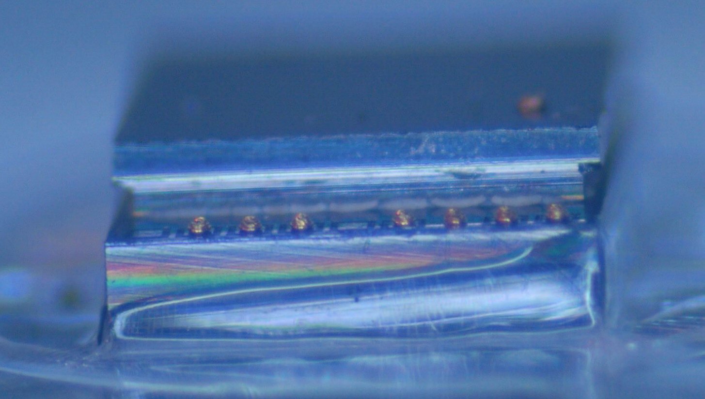
If we etch away the top plastic, we find this two-chip module on the bottom layer. There’s a MEMS chip in the middle and a readout chip on the right, connected to each other by nine bond wires. There’s another bond wire from the top of the MEMS chip to a pin that’s also used by the readout chip, which is most likely the ground pin.
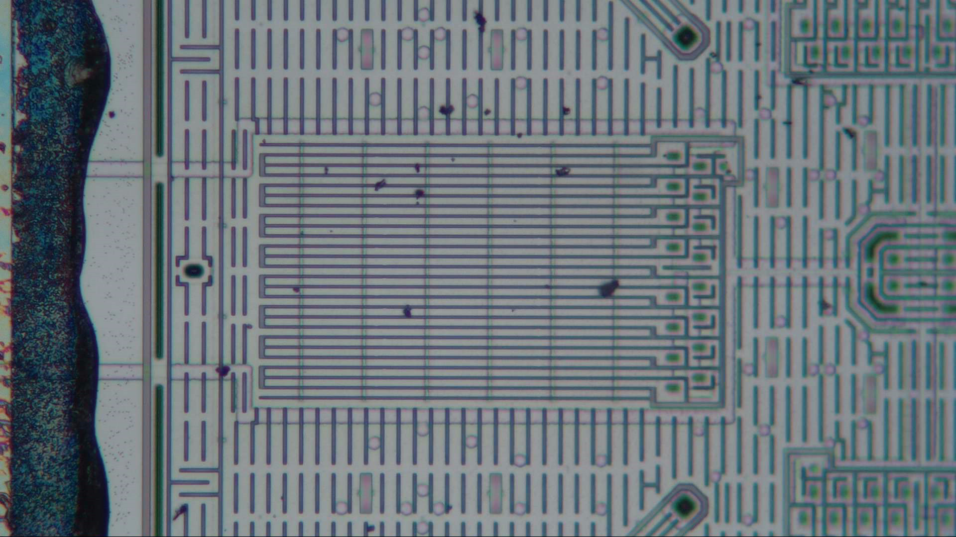
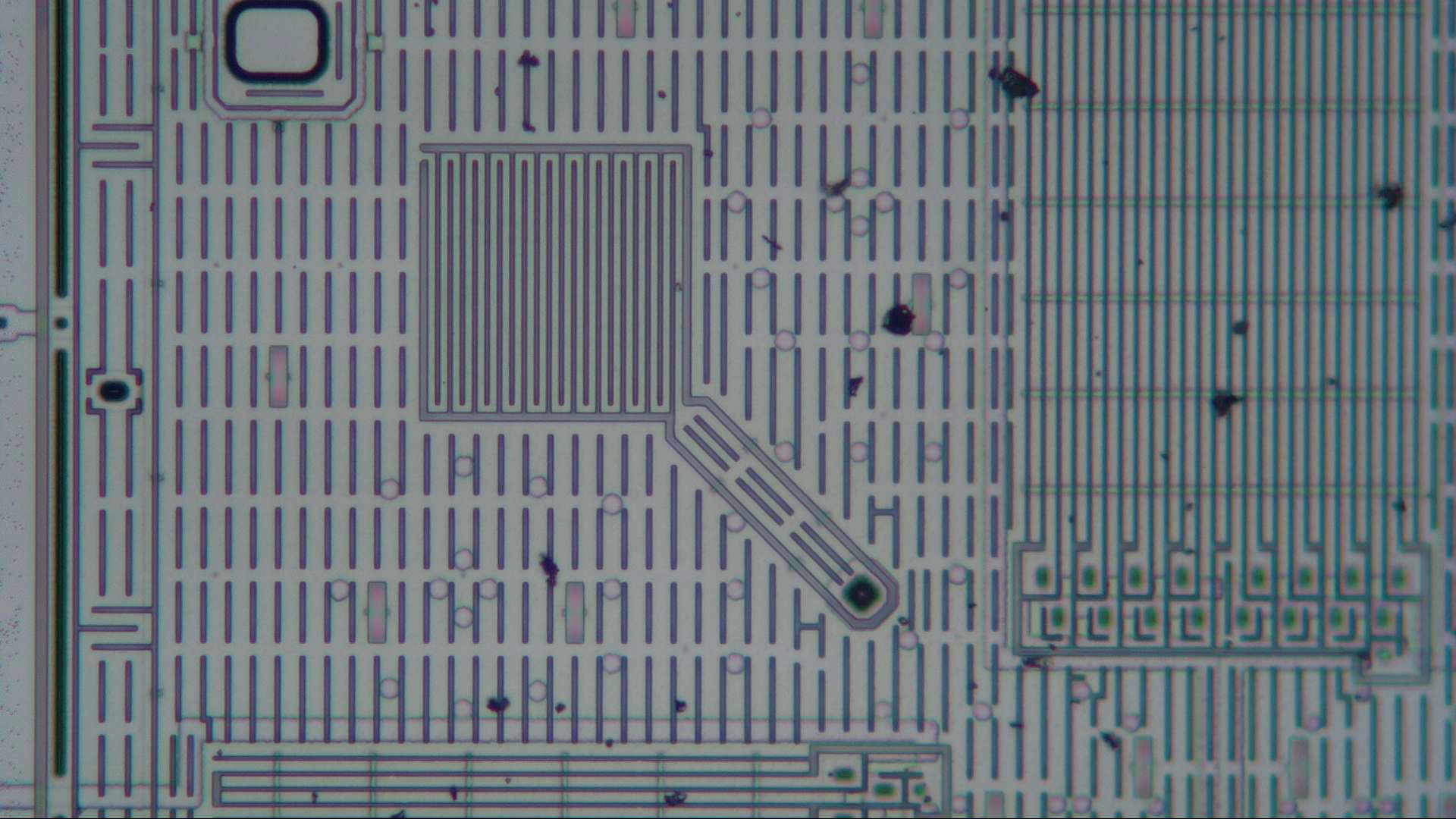
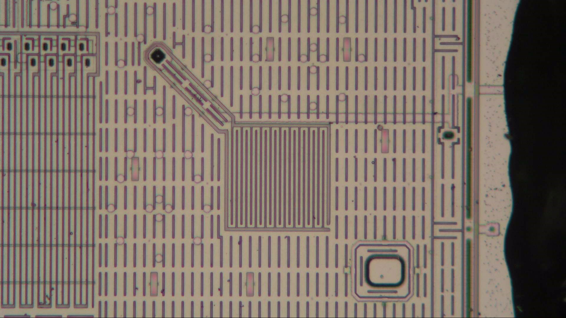
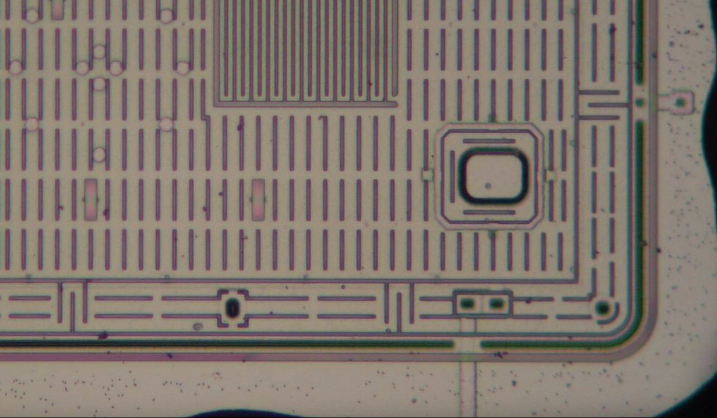
The readout chip is a typical mixed-signal IC. At the bottom there’s a row of bond pads that connect to the MEMS chip, with a three-channel analog-to-digital converter above it. The rest of the chip is a digital engine that drives the ADC, stores the results and sends them out through an SPI or I2C bus.
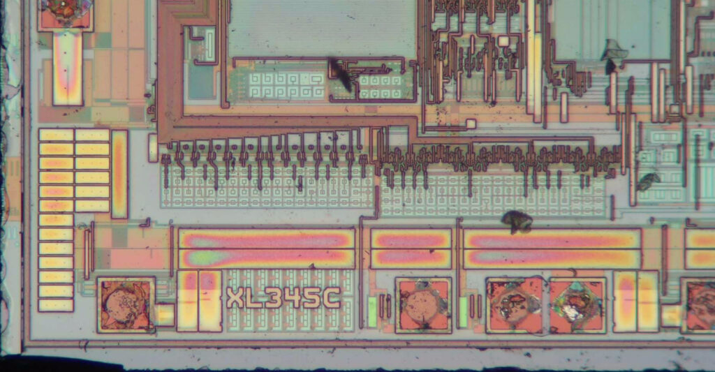
In the bottom-left corner we find the chip ID, confirming that this is an ADXL345.
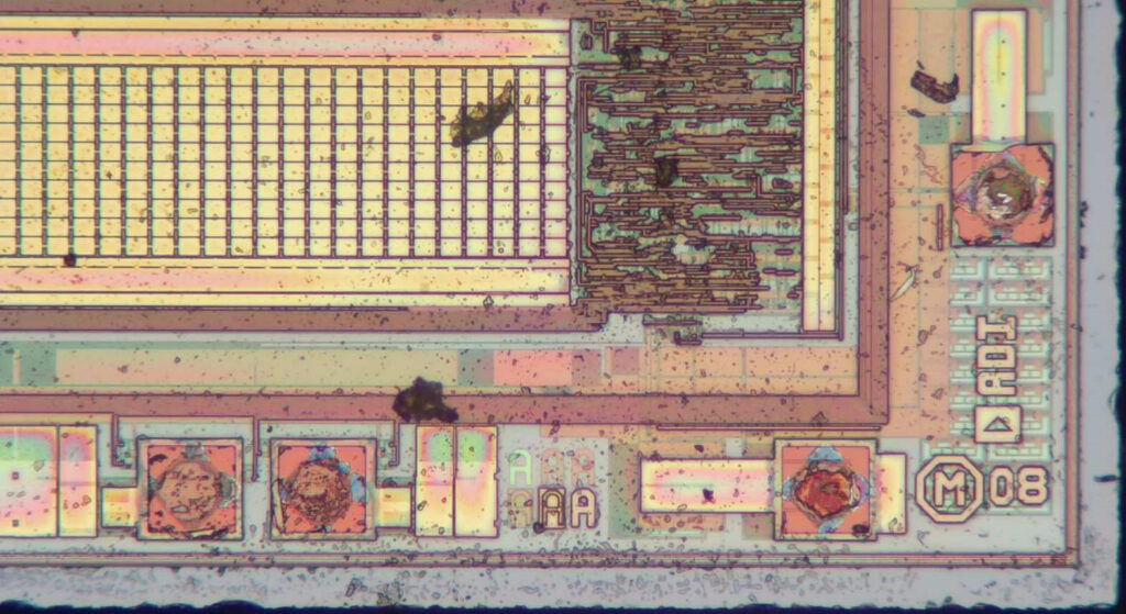
In the other corner are the 2008 copyright date, ADI’s logo and a set of revision letters (all “A”s).
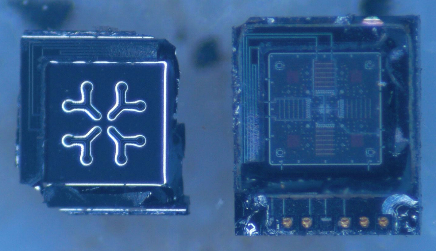
If we take a closer look at the MEMS chip, we find that it consists of two layers of silicon glued together. The top layer (which is in focus on this picture) acts as a protective seal for the MEMS layer below.
For now, we can only see the bond pads of the bottom layer. It also shows a 2007 copyright date and an identifier “ADXL335”. That last bit is interesting: it shows that this chip uses the same MEMS die as the ADXL335, which has an analog output. If that’s the case, then only the readout chip is different between these two products. But then you’d also expect the specifications to be similar, which isn’t the case at all. The ‘335 has a maximum range of +/- 3 g in each direction, while the ‘345 can go all the way up to +/- 16 g. It could be that the limiting factor for the ADXL335’s performance is actually the readout chip, or perhaps ADI found out that the MEMS die could perform with much higher accelerations than initially thought.
The outside is a bit boring however, so we should find a way to separate the two halves. If we look at the stack from the side, we see that the bottom layer is a thick slab of silicon, which probably carries the MEMS structure, while the top layer is a much thinner piece of silicon. The two are glued together through some sort of bonding layer in the middle.
I tried several ways of separating the two without shattering them into a thousand pieces. In the end I found out that I could hold the entire thing sideways and squeeze a sharp scalpel in between the two halves. After carefully applying pressure, the two chips separated cleanly.
Well, relatively cleanly anyway. A few corners were damaged, but the main circuits are still intact.
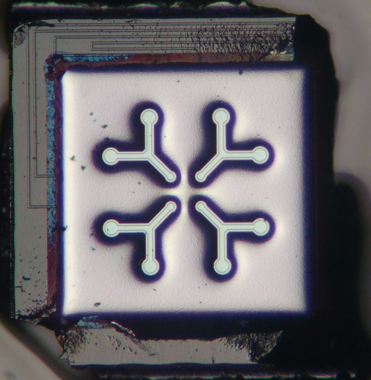
The inside of the top layer has these Y-shaped features. It looks like these would somehow connect to the main MEMS die to act as another connection layer. The wires visible on the edge of this chip are just imprints of the wires on the bottom layer; there’s no other circuitry on the top layer.
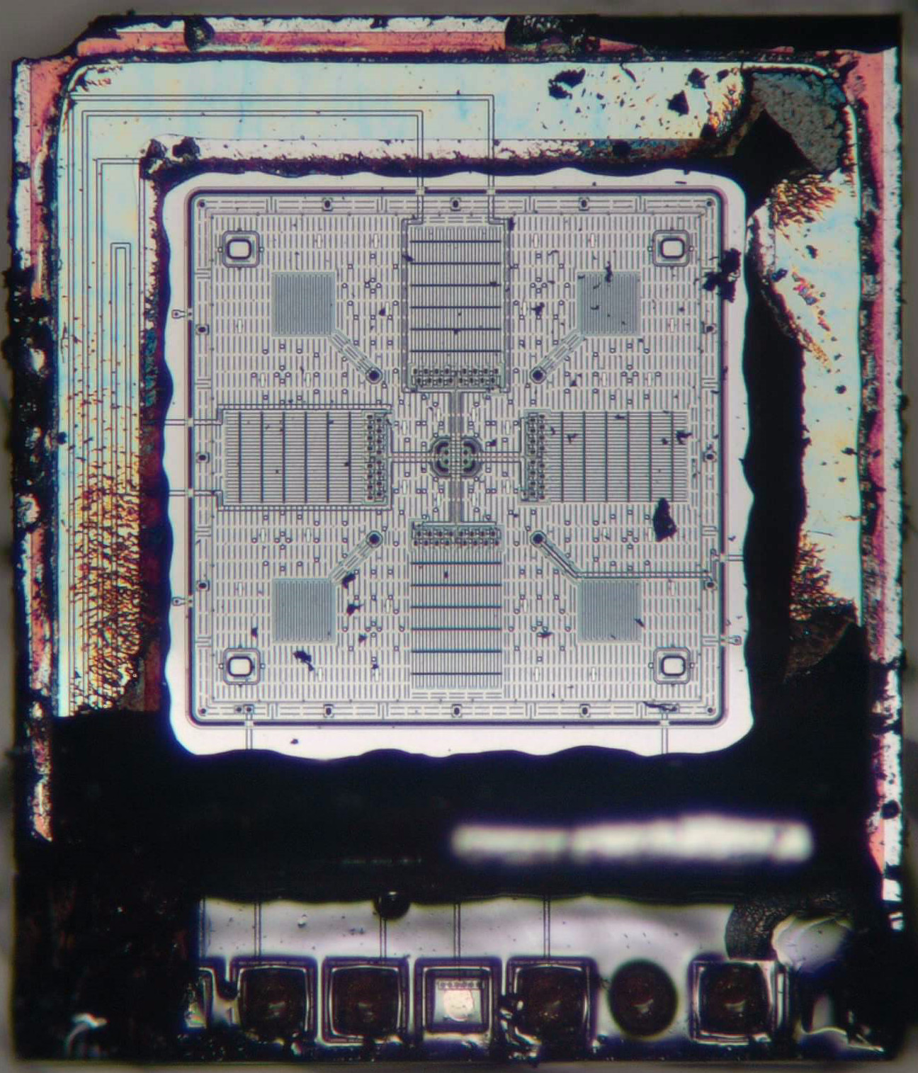
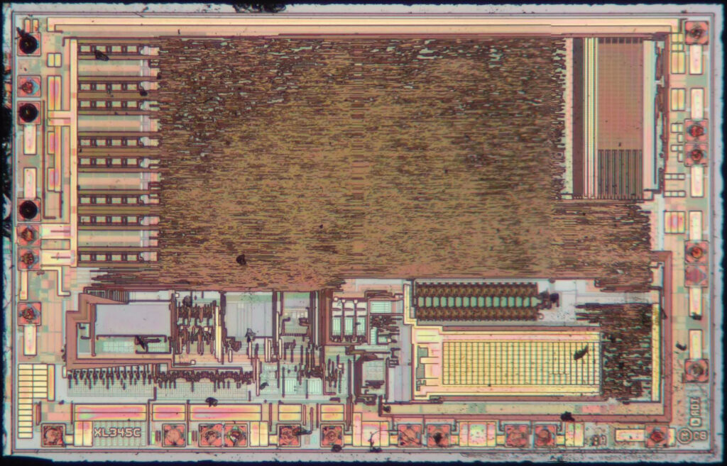
The real magic happens in here. We see a MEMS device in the middle that’s connected to the bond pads through seven lines: two at the top, two on the left, two at the bottom and one on the right. Most of the square device in the middle is the proof mass, which is the bit that moves relative to the chip substrate whenever the accelerometer experiences an acceleration. By measuring the capacitance between the moving part and the stationary part, the chip can determine the amount of acceleration it was subjected to.
The section we see here is used to measure acceleration in the up-down direction. The horizontal beams form an alternating set of fixed and moving beams, arranged in such a way that acceleration in one direction will increase the capacitance between one set and decrease it in the other. The readout chip performs a differential capacitance measurement to figure out how far the proof mass has moved.
A similar structure to measure left-right acceleration is visible on the right of this image. But we also see a square zig-zag structure connected to a 45-degree beam. If you look closely, you also see several small dots arranged in circles. One such circle is just below the square, another is on its right, while a third is just about visible at the bottom (it’s actually clearer on the previous image). These align exactly with the Y-shaped features we found on the top half of the chip that we popped off. Since there doesn’t seem to be any mechanical or electrical connection between the two chips, this makes me think the Y shapes could be bump stops, to prevent the proof mass from slamming into the top chip under heavy acceleration.
As for the square zig-zags, I think that these are the main suspension points for the proof mass. The long zig-zag and the 45-degree beam form a spring that can bend in the left-right or up-down directions. The spring is then anchored to the substrate at the end of the 45-degree beam.
The square zig-zag block on the lower right however, is a bit different because it has a wire coming in from the outside. Since it’s only a single wire, I would guess that this is part of the selft-test function, in which an electrostatic force is applied to the proof mass in order to verify the chip’s functionality. Applying this force in one corner of the chip will pull the mass in a diagonal direction and thereby move it along all three axes at the same time.
The z-axis sensing function seems to be implemented through two wires entering the chip along the lower edge (one is visible here at the bottom right, while the other one is on the left side). As the mass moves up and down, the capacitance between it and the substrate changes, which is detected by the readout chip.
Coming back to the original question, which was why this chip wasn’t functioning correctly, we can at least confirm that the chip inside appears to be the correct one. The most likely explanation is that this chip turned out to be out of spec during production testing and instead of ending up in the recycling bin, was smuggled out of the factory, painted over and re-marked with a different production code. It’s quite normal for a certain percentage of chips to fail, and especially so with a more complex setup consisting of multiple pieces of silicon bonded together in various ways.
In any case, this was a very interesting MEMS chip to look at. There’s a certain beauty in these tiny mechanical structures that’s very different from the complex layouts found in purely electronic chips.
Thanks! Really interesting! I had not spotted the ‘ghost of the previous package marking’, these chips probably have a ‘turbulent past’.