From 1986 to 2008, HP sold a line of workstations and servers powered by a processor line called Precision Architecture, or PA-RISC. These systems were mainly targeted at professional users in industry and academia, and provided high performance at very high cost. Nevertheless, like all computers they became obsolete after just a few years, and I managed to find a heap of old HP equipment in the recycling bin of the local university. Today we’ll have a look at the PA7100 CPU and its accompanying “Viper” memory/IO controller (MIOC), both made in the early ’90s.
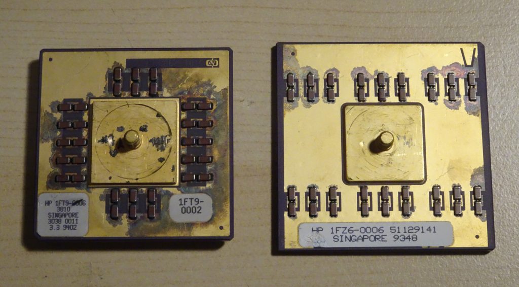
Here we see both chips side by side. The CPU has HP part number 1FT9-0002, although according to the sticker on the left it used to be 1FT9-0006. Not sure what’s going on here… In any case, it’s housed in a large ceramic PGA package with capacitors on top and a screw terminal to attach a heat sink.
The Viper has part number 1FZ6-0006. Its package is similar to the main CPU’s, but slightly larger and with fewer pins.
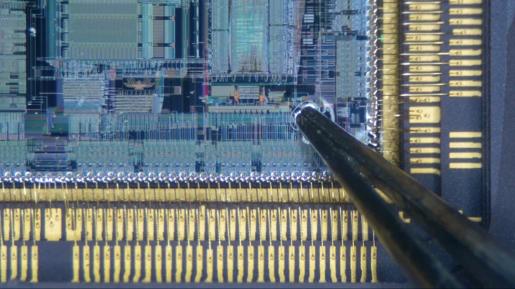
After opening the package we find that the die is covered in a jelly-like substance. I’m not sure what the purpose of this stuff is, but I’d guess to protect the chip from moisture. It does make it hard to take clear pictures of the die, but luckily the jelly seems to dissolve in acetone, and after a bit of rubbing I managed to clean it all off.
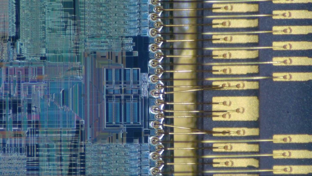
The package has two vertical levels to attach bond wires to. A few pads have double and triple wire bonds, to lower resistance and inductance. These are most likely power and ground.
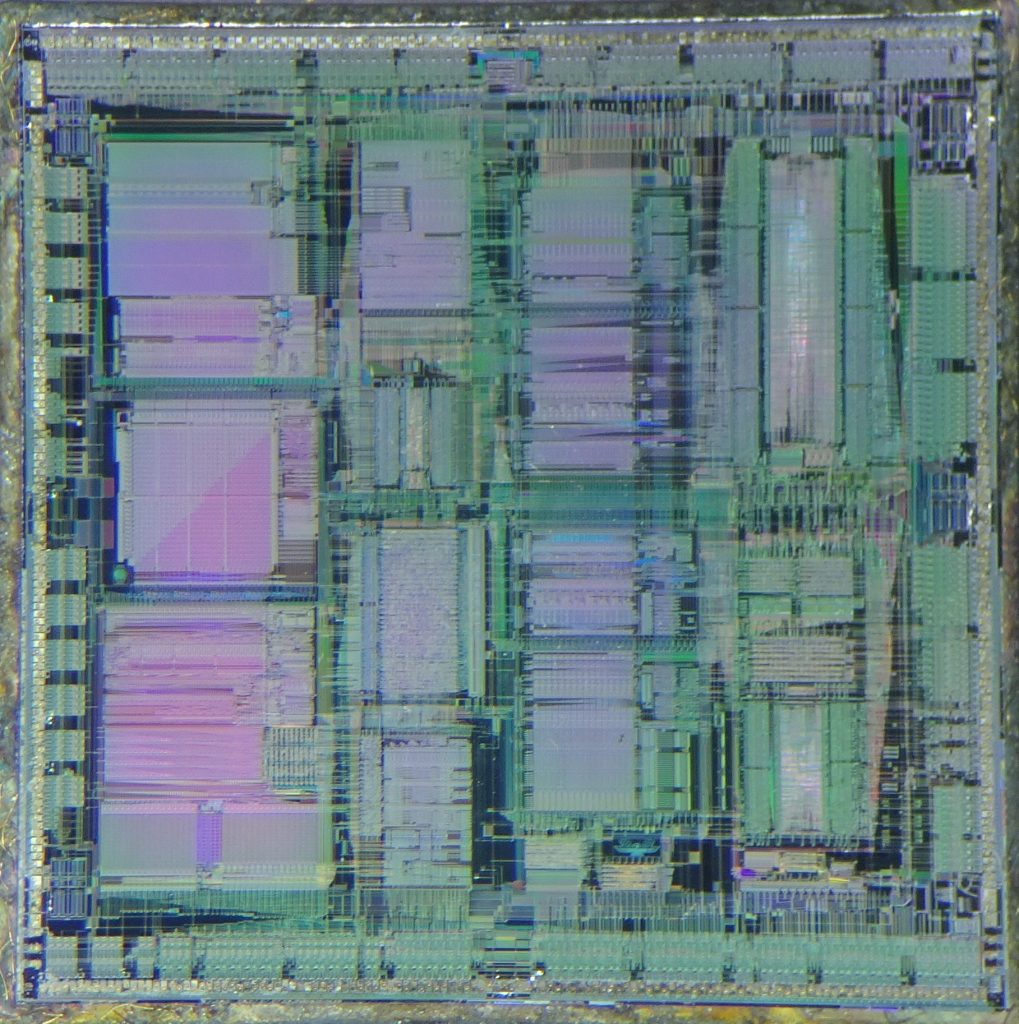
Here’s an overview of the complete die. It contains the CPU core as well as an FPU, an MMU and a cache controller. It’s made in a 0.8 micron process [1]https://www.openpa.net/pa-risc_processor_pa-7100.html.
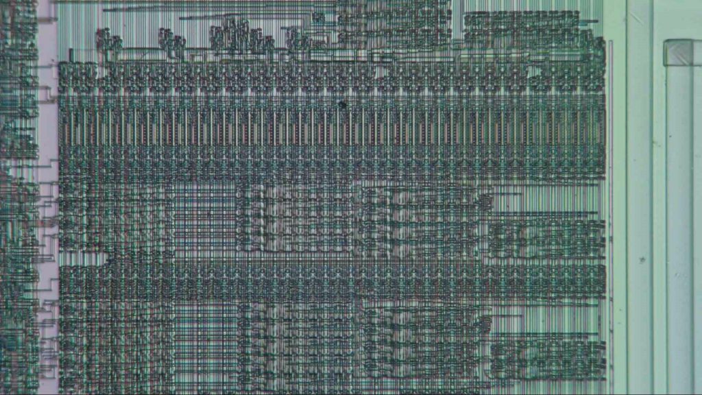
Zooming in on one piece of digital logic.
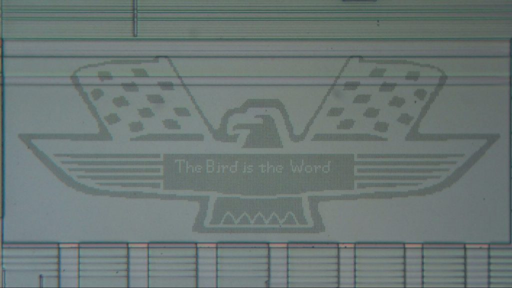
The old HP company was famous for including chip art on its designs, and the PA7100 is no different. “The Bird is the Word” is a lyric from the 1963 song Surfin’ Bird by The Trashmen.
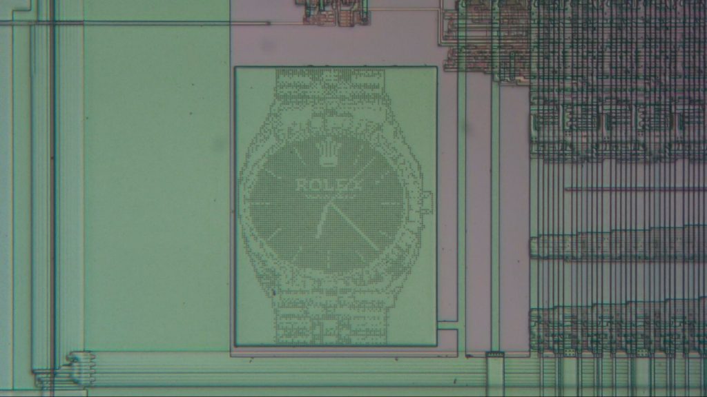
Another doodle is this very detailed Rolex watch.
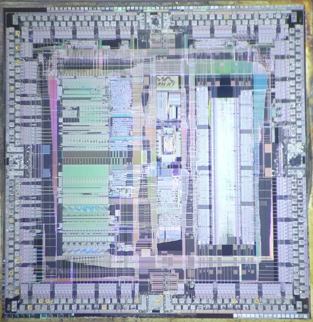
The Memory and I/O Controller, or MIOC, manages the flow of data between the CPU, the memory and peripheral devices. This one has code name “Viper” and is part of the ASP chipset. Like the CPU, it’s made in a 0.8 micron process [2]https://www.openpa.net/pa-risc_chipsets_asp.html.
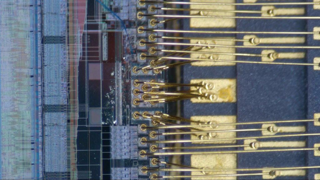
The Viper’s power and ground pins are attached with up to eight bond wires on a single pad! It’s amazing how they managed to make this fit, and I can’t imagine it was cheap.
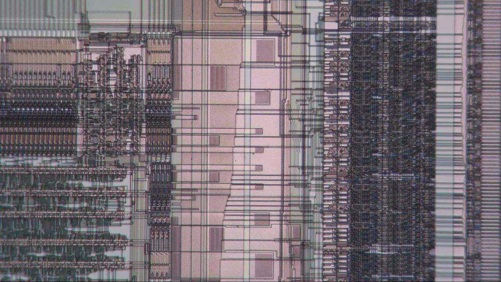
The circuitry looks similar to that of the CPU. Wide power lines and large data buses are visible.
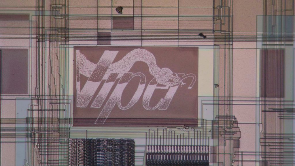
Again, we find examples of chip art. This is apparently the logo of the Viper project.
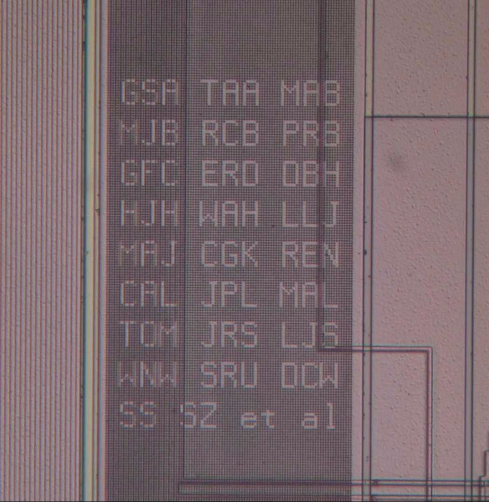
These are the credits of the design team. It’s not easy to figure out who these people are; I found an old paper [3]https://web.archive.org/web/20101207043600/http://www.hotchips.org:80/archives/hc4/2_Mon/HC4.S2/HC4.2.1.pdf that describes the PA-RISC architecture written by Syrus Ziai, Tom Alexander and others, so perhaps that explains SZ and TAA.
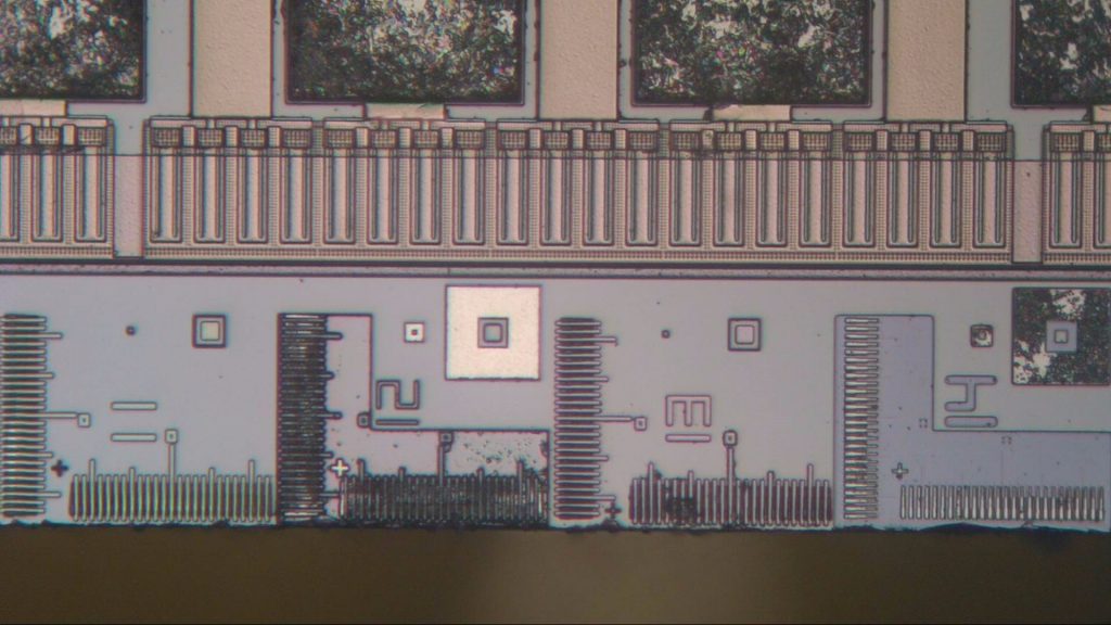
On the edge of the die we find these test structures. There’s one for each of 14 layers, and the little rulers are used to check the correct alignment of each layer with respect to the previous ones.

“If you can read this…. you are too damn close!” written in tiny little letters. Again, typical HP humour.

Great work! I assume that the CPUs are tested at different clock speeds and the higher the part number, the higher the frequency. Once a CPU fails, it is downgraded to a lower number. I saw this in various published pictures.
Anyway, it is my current hypothesis…
Hi CPU Duke! I think what you’re referring to is frequency binning.
This is common practice in CPU manufacturing because despite it being an extremely high-precision process, there’s still so much inherent variability that the resulting products can be significantly different from one batch to the next. This is especially true for brand-new production processes, because the manufacturer hasn’t yet had the opportunity to fine-tune every step.